Intel Corporation (INTC)
A mighty history but an uncertain future (?)

This is the second of a series of longer articles on the chip industry. We have already written about Taiwan Semiconductor and Broadcom as part of this round.
Any review of the chip industry is not complete without considering Intel (INTC). The company has been a great powerhouse and included legendary figures such as Andy Grove, Gordon Moore and Robert Noyce in its ranks.
The key question is Intel’s past more glorious than its future?
We will consider aspects of the history of the company before taking a more detailed look at the current situation.
Introduction
Vacuum Tubes vs Transistors
The modern world is run by billions of transistors found in all types of electric devices. They are the atoms of modern-day computing, combining to create the “logic gates” that enable computation. The invention of the transistor in 1947 opened the door to the modern information age.
The computer pre-dates the transistor. Early computers such as the ENIAC (see below) were rudimentary systems which took up entire rooms and weighed thousands of pounds and were made up of vacuum tubes. Vacuum tubes are based on a phenomenon called thermionic emission where heating a metal knocks some electrons loose.
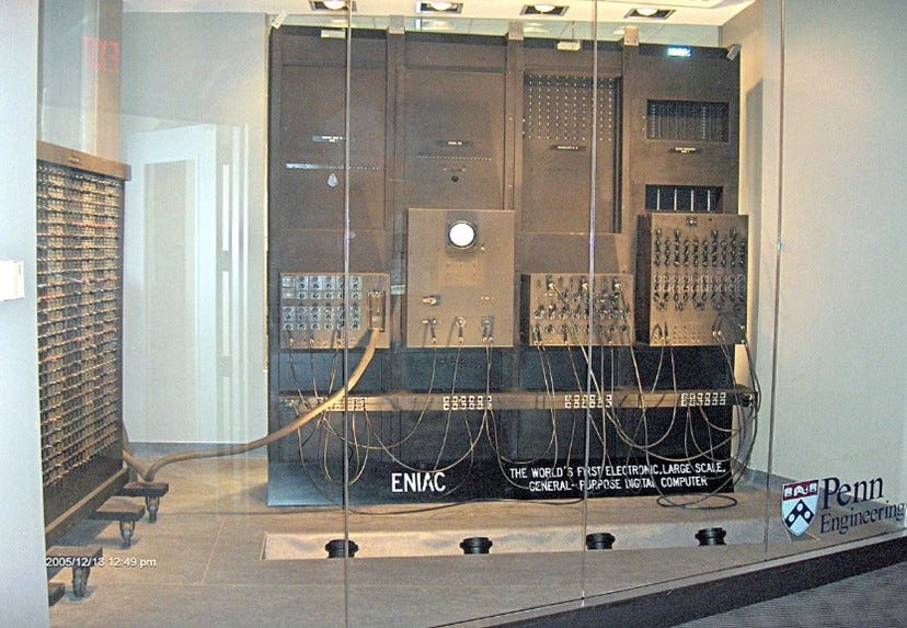
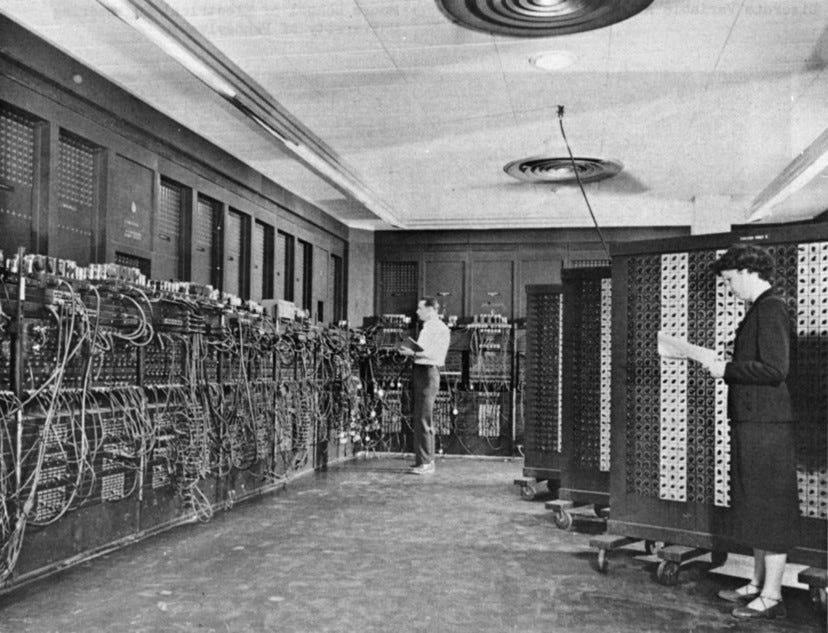
The ENIAC (Electronic Numerical Integrator and Computer was made in 1945 at the University of Pennsylvania. Source Wikipedia.
In 1904, English physicist John Ambrose Fleming created the first vacuum tube device. The basic device is shown below
When the cathode is heated, and a positive voltage is applied to the anode, electrons flow from the cathode to the anode. This type of device with just two electrodes is called a diode. Electrons can only flow from the Cathode to Anode.
In 1907, American inventor Lee de Forest added a third electrode to create the first triode tube. The triode can be used as an amplifier of electric signals whereby a small change in grid voltage leads to large change in the plate current.
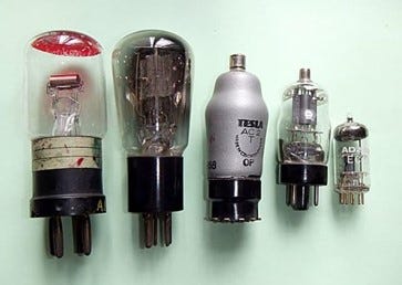
The evolution of triode vacuum tubes from a 1916 model (left) to the 1960s. The middle one is called Tesla. Image source: Wikipedia
Vacuum tubes were used for a long time, but they had limitations. They were relatively large, prone to periodic failure’ necessitating replacement, and they got hot as the filament need to be heated. Therefore, computers using vacuum tubes had to be very large, to facilitate cooling and tended to be unreliable.
In 1947, William Shockley, Walter Brattain and John Bardeen created the world’s first transistor at the legendary Bell Labs. The transistor replicated all the functions of vacuum tubes, like switching and amplification, but was made from semiconductor materials such as silicon. The invention of the transistor marked the end of the vacuum tube.
“A semiconductor material has an electrical conductivity value falling between that of a conductor, such as metallic copper, and an insulator, such as glass. Its ability to conduct electricity rises as its temperature rises; metals behave in the opposite way”. Wikipedia
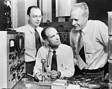
John Bardeen, William Shockley and Walter Brattain developed the bipolar point contact transistor in 1947. Image Source: Wikipedia

William Shockley. Image Source: Wikipedia
Over the next three decades, scientists worked on improving the quality of transistors. William Shockley moved to Mountain View, California, won the Nobel Prize in Physics and started Shockley Semiconductor Laboratory – the first entity working on semiconductor devices in an area which later became known as Silicon Valley.
Shockley was adept at recruiting brilliant engineers but terrible at managing them due to his domineering and paranoid manner. In late 1957, eight of his engineers, including Gordon Moore and Robert Noyce left to join a new start up called Fairchild Semiconductor. In the next 20 years, more than 65 new semiconductor companies were started by employees who left Fairchild Semiconductor.
The development work now focused on Integrated Circuits (IC) (a device which integrated semiconductor devices such as transistors and diodes and passive devices such as resistors and bonded them on a Printed circuit board (PCB)). Robert Noyce invented and patented a new IC using silicon in 1958.
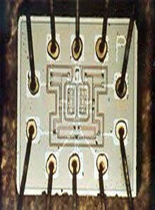
Robert Noyce monolithic Integrated Chip invented in 1958. Source: Wikipedia.
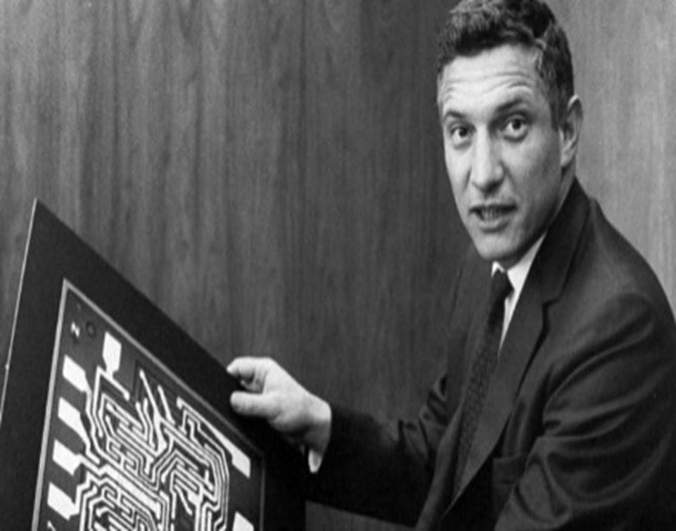
Robert Noyce with an expanded drawing of his 1958 chip. Source: Wikipedia.
Intel Inc: The start-up pioneer which became a colossus
Intel Inc was founded on July 18, 1968, by Robert Noyce and Gordon Moore. It was financed by Arthur Rock who was the first Silicon Valley venture capitalist and investor. The third employee was Andy Grove, a Hungarian Jew who had arrived in the United States in 1956 at the age of 20 having seen the terrors of both the German Nazis and the Communists in the land of his birth.
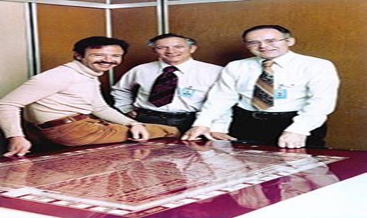
Andy Grove, Robert Noyce, and Gordon Moore (1978). Image Source: Wikipedia

Intel’s first Chip-the Intel 3101. Image Source: Wikipedia
The Intel 3101. This was Intel’s first product and was the world’s first solid-state memory chip. Before 1968, no memory chips existed. The 3101 used miniature semiconductor transistors in place of the bulky magnetic cores. The 3101 brought greater speed, less maintenance, less bulk, and less heat to mainframe computers. It had 2000 transistors and had as much power as the 1946 ENIAC computer. For the first, ten years Intel’s main business was providing memory chips for mainframe computers.
Noyce and Moore were brilliant engineers but business success in the complex chip manufacturing business depends greatly on reducing the wastage percentage: the proportion of chips rejected as faulty. Grove who had continued to teach on chip design, while working at Fairchild Semiconductor, had written a college textbook on the subject. Grove was in charge of manufacturing.
Grove was the de-facto CEO of the company long before he was officially elevated to that position. In 1983, he wrote a book, High Output Management, in which he described many of his methods and manufacturing concepts.
He was an intense, hard-driving, methodical manager who had little time for small talk and did not suffer fools gladly. He was always fearful competitors would use invention, innovation, and engineering to destroy Intel.
Grove is perhaps best known by the public for his summary of his business philosophy which was also the title of a book he wrote: “Only the Paranoid Survive”.
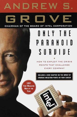
Cover of Grove’s book. The full quote was “Success breeds complacency, Complacency breeds failure, only the paranoid survive.” Source: GoodReads.com
Intel had invented the microprocessor as early as 1971. The 4-bit Intel 4004 was followed by several improved versions which ended with the 32-bit Intel 80386 in 1985, almost 30 years ago. This defined the baseline x86 architecture that is in modern processors in most laptops, desktops, and servers today.
The pace of development was relentless. The 80386 was succeeded by the 80486 and the Pentium. Every release made computers so much faster that use cases, unimaginable only one or two years prior, were suddenly possible.
These chips are called logic chips. Logic chips are the 'brains' of electronic devices – they process information to complete a task. Among Logic chips, CPUs (central processing units) are the 'original' chips, first designed in the 1960s. Graphics Processing Units (GPUS) are also logic chips. The other main other types of chips are memory chips which are designed to store information.
A summary of process of manufacturing chips is shown in the chart below
Moore’s Law

Gordon Moore in 2004. Image Source: Wikipedia
In an article in 1965, Gordon Moore had forecast that the number of components that could be packed into an integrated circuit would double every year (later changed to every two years) for at least a decade with no increase in power consumption). His revised forecast implied a compound annual growth (CAGR) of 41%. While Moore did not use empirical evidence in forecasting the historical trend would continue, his prediction held since 1975 and has since become known as a "law".
“The complexity for minimum component costs has increased at a rate of roughly a factor of two per year. Certainly, over the short term this rate can be expected to continue, if not to increase. Over the longer term, the rate of increase is a bit more uncertain, although there is no reason to believe it will not remain nearly constant for at least 10 years.[1] “ Gordon Moore 1965
It was a remarkably accurate forecast which, if anything, proved to be too conservative. When Moore wrote his article, the best chip would have about 50 transistors. The chart below shows the 50 year semi-log plot of the number of transistors on a chip. It is a remarkable straight line indicating the exponential growth of the transistor count and thus the power of chips. The number of transistors has increased from 1000 in 1970 to 50bn in 2020. This was a growth of 50,000x over 50 year span. Moore’s law ( doubling every two years ) would have predicted a 33,500 x increase ( 2^25). The actual improvement in chips over fifty year was greater than predicted by Moore’s law.
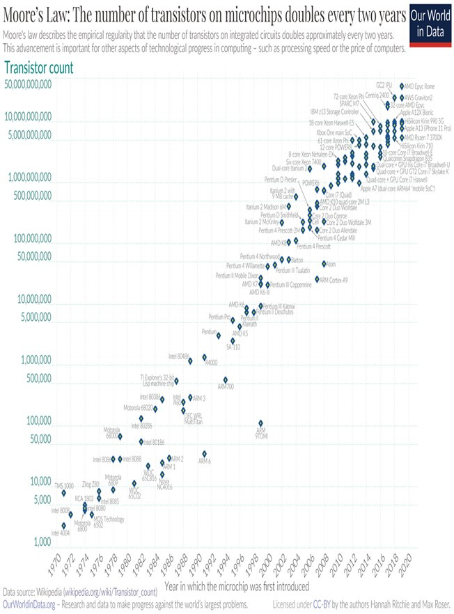
The chart above explains the evolution of computer technology in the last 50 years. The power of computers has grown exponentially, and the size of chips and their prices have fallen equally dramatically. The range and quality of electronic devices has changed completely in the last 50 years. It is often said that the smartphone in your pocket is millions of times more powerful than the Apollo 11 guidance computers used by NASA to send man to the moon in 1969. These changes have boosted economic growth, productivity and completely transformed economies and societies.
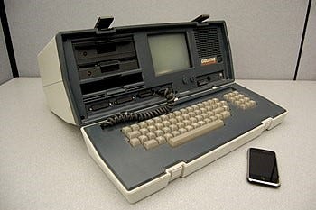
An Osborne Executive portable computer from 1982 (4MHz CPU from Zilog) and 2007 Apple I-Phone (with 412 MHz ARM 11 CPU). The former has 100X the weight, 500X the volume, 10X the inflation adjusted cost, and 1/100 the processor speed of the Apple phone. Image and text source: Wikipedia
In nature, in business and in financial markets, exponential growth does not last forever and there is tendency to revert to the mean. Some constraints always come in to reduce the rate of growth. In recent decades, there have been countless articles about the end of Moore’s Law.
In 2005, Moore wrote “In terms of size [of transistors] you can see that we're approaching the size of atoms which is a fundamental barrier, but it'll be two or three generations before we get that far—but that's as far out as we've ever been able to see. We have another 10 to 20 years before we reach a fundamental limit. By then they'll be able to make bigger chips and have transistor budgets in the billions”
A headline in March 2024 was as follows: “Cerebras Systems Unveils World’s Fastest AI Chip with 4 Trillion Transistors.”
The first type of limit is driven by the laws of Physics. As chips get smaller, further miniaturisation gets more difficult to achieve, especially as work is now being done at sub-atomic levels.
The second was described by Arthur Rock, the original Intel investor and long-time Director, as Moore’s second law. This states “the cost of a semiconductor chip fabrication plant doubles every four years”. As chips grow smaller and more powerful, the capital cost of putting up a Chip manufacturing grows exponentially. hip manufacturing has always been a capital-intensive industry: an investment of US$ 10bn-20bn is required for setting up a new leading-edge plant today.
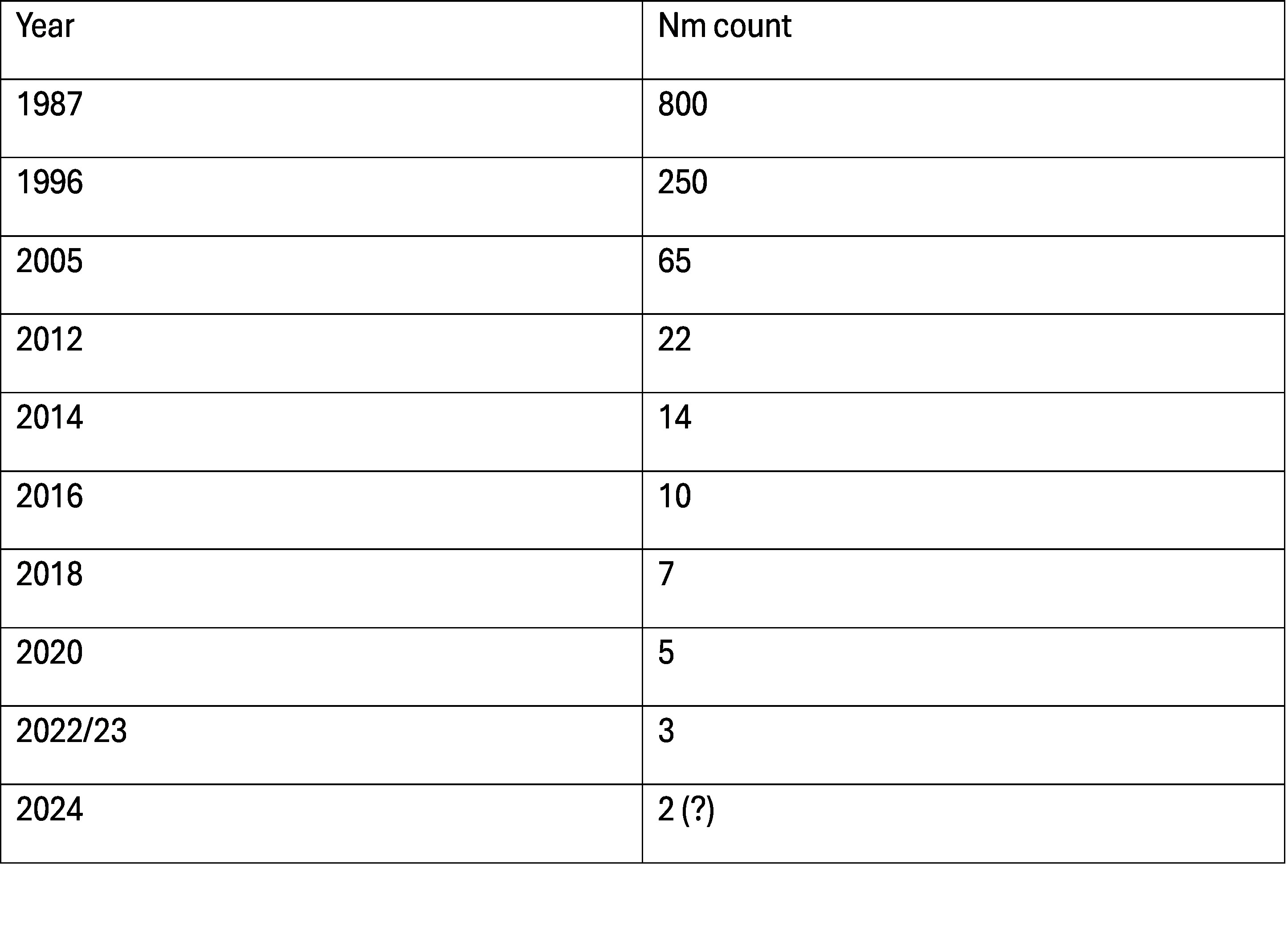
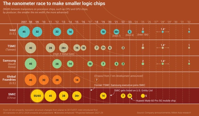
If more and more transistors must be packed onto a chip, the transistor must get smaller. The key metric in this area is the nanometre (nm). A nanometre is one billionth of a meter (!), also expressed as 0.000000001 or 10-9 meters (for perspective, hair grows at roughly 1 nm per second).
In chip design, Nanometre refers to the width of the gate on transistors. Smaller gates allow more transistors to be squeezed into the same area of silicon, enabling more powerful processors. The smaller the size, the more challenging and expensive the chip is to produce but the more processing power that can be packed into a given space. The reduction in nm in the last 35 years has been remarkable as shown below:
Beyond Moore’s Law
In a world in which most forecasts fail after a few months, Moore’s Law has proved remarkably prescient for many decades. However, the physical limitations to it have been biting strongly and new approaches are needed if the powerful chips required in the Fourth Era of Computing are to be delivered
New approaches
Future innovation will require new approaches and new thinking. One of the key challenges of engineering future nanoscale is the design of gates. As device dimension shrinks, controlling the current flow becomes more difficult. Even when the gate is turned off, because they are so close to each other, there is some electron “leakage”.
Modern transistors take the form of a Multi-gate device – i.e., many (ever smaller) gates on a single device. They are called MOSFETs (multi-oxide-semiconductor field effect transistors) and were first invented in 1959. Researchers have been developing MOSFETS to slowly extend Moore’s Law in the last 50 years.
Until 2012, transistors were laid flat on the surface or plane of a semiconductor: that limited the number of transistors that could be packed in an area. This was called planar transistor architecture.
In 2016 , the FINFET 3d structure was devised and this was followed by Intel’s RibbonFet. The video below gives some information on these innovations.
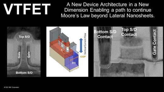
However, all these were still planar. In December 2022 researchers at IBM and Samsung announced a chip 'breakthrough' that could extend the life of Moore's Law by a few more years. This has a new Vertical Transport Field Effect Transistors (VTFET) design, which lays transistors perpendicular to the surface of the chip, allowing a vertical current flow. Researchers believe vertical packing could help to pack more transistors and reducing energy usage by as much as 85%. This might lead to, for example, smartphones that are only charged weekly.
A more radical approach might involve photonics, the science of light waves, to build chips.
Photonic ICs use photons rather than electrons to process and distribute information. In an electronic chip, electrons pass through electrical components such as resistors, inductors, transistors, and capacitors; in a photonic chip, photons pass through optical components such as waveguides, lasers, polarizers, and phase shifters.
Proponents argue that photonics can result in large speed improvements along with reduced power consumption. If this proves to be correct, Moore’s Law could be extended for a couple of decades more.
Intel : The rise of the desktop PC
Although Intel’s brilliant engineering led to huge advances in microprocessors, in the first 15 years, the bulk of its revenue in the early years that time came from supplying to memory chips for mainframe computers.
In the mid-1980s, Andy Grove and Intel made the difficult decision to pull out of the Memory Chip business due to intense competition from Japanese companies such as Toshiba, NEC, Hitachi, Matsushita, Mitsubishi etc. There was overcapacity, and these companies were selling below cost price in global markets. Grove correctly decided that the PC CPU business was a better bet.
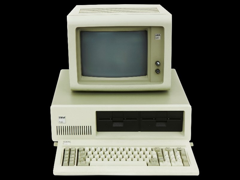
The IBM PC, introduced in 1981, helped to reassure corporate customers that small computers were a serious idea and not just for hobbyists and science students. Image source: Wikipedia
In 1981, IBM created its PC and decided to install Intel x86 processors in them. IBM had forecast demand for 1mn over three years with 200k in the 1st year. In fact, by the 2nd year, they were selling 200k a month. IBM stumbled in their designs and “clone makers” such as Compaq, Gateway and Dell prospered. Buyers realised that clones were just as good if not better than IBM machines if they had Windows Software and Intel Chips (“Wintel”). Intel promoted the advertising slogan “Intel Inside” directly to the consumer to suggest the brand of the machine did not matter if it had “Intel Inside”.
By the end of the 1990s, Pentium (Chips now had names rather than numbers to better appeal to the end-consumers) processors invented by a team led by Vinod Dham had become a household name.
The first Pentium, which contained two processors on a single chip and approximately 3.2 million transistors was introduced in 1993. Pentium was the first Intel chip for PCs to use parallel processing, enabling significant increases in speed and efficiency. It was the first chip that enabled consumers to use PCs for serious gaming, as older chips did not possess the processing power capable of maintaining video game graphics
There were huge advances in Pentiums in the 1990s. The Pentium Pro in 1995, the Pentium II in 1997, the Pentium III in 1999, and the Pentium 4 in 2000
In two or three decades, the PC and laptop market grew exponentially, and the PC standard dominated (Apple Computer had a tiny market share). Intel grew strongly on the back for this. The company was so dominant that it and Microsoft (“Wintel”) faced accusations of abusing monopoly power.
Intel had become a global enterprise with manufacturing operations in Malaysia, Israel, and Singapore as well as the United States. However, it had a much larger US manufacturing blueprint compared with its rivals. After 2000, the demand for PC microprocessors slowed and Intel lost some market share to competitors such as AMD. Intel tried to diversify its business beyond PC chips but few of these activities were ultimately successful.
Between December 1989 and 2000, Intel’s stock price rose by a 43.2% per annum (CAGR) giving a total return of 3860%. In the 2000 technology boom, the price peaked at $ 75 per share before crashing to below $ 13 in 2002. The golden days were over and even today, the stock trades at $ 30 per share.
For the last 35 years, INTC has given a CAGR return of 12% which is broadly in line with the S&P 500 Index. In the last ten years the CAGR return is just 3.8%. Intel has a great history, but something has gone badly wrong in the last five years.
What went wrong?
We will summarise the reasons before considering them in detail.
Intel had prospered greatly as the dominant designer and manufacturer of x86 architecture-based CPUs for Personal Computers (PC) and servers. However, various developments after from 1995 onwards combined to show the limits of Intel’s dominant position.
The mobile revolution was a huge global phenomenon especially after the introduction of the Apple iPhone. Intel was at best a minor supplier of chips for mobile devices. The space was dominated by companies such as Samsung, Qualcomm and Broadcom. Intel missed out on mobile.
The rise of TSMC as specialist third party manufacture encouraged new Fabless chip companies such as Nvidia, Qualcomm, Mediatek, etc who designed chips but outsourced manufacturing to companies such as Samsung and TSMC. Intel did not manufacture for outsiders in a big way. Intel missed out on the 3rd party manufacturing business.
Intel focused on CPUs and paid less attention to GPUs. Nvidia become the dominant GPU supplier feeding demand from Gaming, Cryptocurrency Mining and new Gen AI datacentres. GPUs has rapidly grown to become a $ 100bn a year plus opportunity dominated by Nvidia. Intel has missed out on the GPU boom.
Many new chips such as those developed by Qualcomm, Apple, Alphabet, Amazon, Meta and new Chinese companies are based on ARM or the open-source blueprints rather than x86. This growth has bypassed Intel.
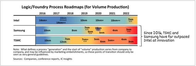
Even in the core x86 space, AMD which had been an also-ran for twenty years improved its products after 2012 when current CEO Lisa Tsu took the helm. AMD has increased its CPU market share significantly in PCs after introducing its Ryzen chiplet architecture in 2017. Intel still leads in Laptops and Servers.
Let us consider all these factors in detail.
Mobile failure
PCs sells in the hundreds of millions – smartphones sell in the billions.
Intel dominated the supply of chips in the former but never made it into the latter. Instead. the prize went to Samsung, Qualcomm, and TSMC.
In PC Chips, the success that Intel achieved was its ability to both effectively design and efficiently manufacture ever faster chips. In the case of smartphones, efficiency in power management is of greater importance. Intel was too focused on speed and not enough on power management to even be in the running for the iPhone CPU, and despite years of trying, couldn’t break into Android either.
This meant huge, missed opportunities and significant foregone revenue and cashflow. This loss of cash was a major problems. Over the last two to three decades, the cost of building ever smaller and more efficient processors has risen exponentially. Companies looking to manufacture leading edge chips needed greater and greater revenues and cash flows to invest in new capacity.
A major source of increased revenue has been billions of smartphones sold over the last two decades decade; Intel had not seen any of that . PC sales grew much more slowly than mobile.
The smartphone growth explosion which followed the introduction of the iPhone permanently relegated x86 computer chips to a small minority of the overall computing market
Server Success
In the 1990s and early 2000s, Intel was rapidly improving performance while reducing prices as PC demand exploded. The Server space was dominated by Sun Microsystems which had the Solaris range of Integrated Servers powered by its Java language. Sun was acquired by Oracle Inc in 2009.
PCs didn’t match the reliability of integrated servers, but their chips were improving. Google was expanding its network of datacentres as demand for its search engine (first introduced in 1998) was exploding with the parabolic growth of the internet. In the early 2000s Google realized that the scale and complexity entailed in offering its service meant that building a truly reliable stack was impossible; the solution was to build with the assumption of failure, which in turn made it possible to build its datacentres on lots of (relatively) cheap x86 processors. Intel was the dominant producer and supplier of these. Google’s approach was adopted by every major datacentre operator, and x86 chips became the default chips set for servers.
The demand for servers was greatly boosted by the growth in cloud computing. This was pioneered by Amazon in 2005-07. About 7-8 years later Microsoft, Google, IBM, Alibaba, Oracle and others also began investing in the sector.
Intel made the best x86 processors, particularly for server applications. AMD occasionally threatened the incumbent on the desktop, but usually at low end and was rarely considered for Servers.
The rise of 3rd party Manufacturers.
We recently wrote a note on Taiwan Semiconductor (TSMC) which can be seen here. we noted Morris Chang founded TSMC in 1987 as a pure play chip foundry which would manufacture chips for external players. TSMC was a great success on its own terms. It encouraged the formation of new companies which were “pure-play designers” with no manufacturing capacity.
Nvidia, Qualcomm, MediaTek are among many companies founded after TSMC, whose business models only made sense due to the pure-play model pioneered by TSMC. AMD sold off its foundry operation and that subsequently became Global Foundries.
The fabless companies are happy to focus on higher margin design work. They have left the manufacturing to specialists such as TSMC, Samsung, Global Foundries and Intel.
Effectively the Chip world has bifurcated, and Intel is in the uncomfortable position of being an integrated player in a world of specialists. An Integrated Devices Manufacturer (IDM) encompassing both design and manufacturing.
Samsung is an IDM too, but it produces a chips for its own successful consumer devices such as phones, tablets and consumer electronic products. Unlike Intel, Samsung has ridden the mobile chip wave and supplied chips for Apple phones despite being a competitor.
Most mobile chips are centred on blueprints provided by ARM Computers. For the cost of a license fee payable to ARM, a company like Apple, Google Meta, Amazon or Microsoft can create their own modifications, and hire a foundry to manufacture the resultant ARM-based chip. The designs are unique in small ways, but design in mobile will not be dominated by one player in the way Intel dominated PCs.
Apple used ARM blueprints to create its M1 and M2 chips. These 5nm chips had excellent performance metrics and were manufactured by TSMC. The M1 and M2 chips displaced Intel chips in Apple Macs. This reflects both the quality of Apple’s design prowess and TSMC’s leading-edge 5nm manufacturing .
There are now many potential competitors to Intel in both the design and manufacturing space.
TSMC worked with Apple and Qualcomm and others to make the huge volumes of chips demanded by the mobile revolution and used the cash to invest heavily and work with companies such as ASML to surpass Intel’s manufacturing capabilities.
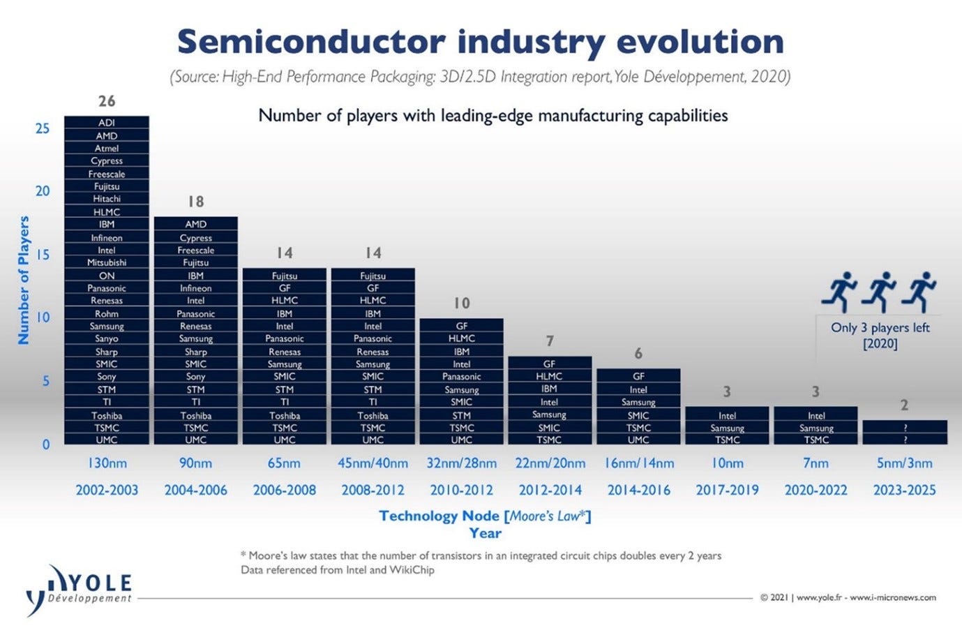
Leading edge manufacturing capability is increasingly rare: only about four of five companies at most can make leading edge chips (7nm or lower). Only two companies could make 5 nm chips after INTC failed in 2020 at the 7nm stage leaving just TSMC and Samsung. This was stunning setback for a company known for its engineering prowess.
These developments means INTC faced various threats on both design and manufacturing
AMD
AMD chips were now faster than Intel on the desktop, and very competitive in the datacentre. AMD is no longer an also ran. It improved its designs but also benefited from the fact that it was manufacturing chips on TSMC’s 5nm process.
Nvidia and GPUs
While CPUs have been a significant revenue stream for Intel, the evolving landscape, characterized by shifts towards GPUs, AI accelerators, and foundry services, signals the necessity of diversification. Nvidia is the dominant player in GPUs. Its chips are manufactured mainly by TSMC.
Other Chip designers
Large Cloud Service Providers (CSPs) are increasingly investing in their own chip designs; Amazon, for example, is on the third iteration of their Graviton ARM-based processors and these are also manufactured by TSMC.
These trends favour TSMC and reduce the opportunities for Intel in 3rd party manufacturing. As we highlighted in our note, TSMC has not stopped investing or investing. In the last five years it has invested over $ 150bn. This huge investment is only going to increase TSMC’s lead over INTC.
Intel needs manufacturing volumes to generate cash and one way to get that would be to manufacture for others. However, TSMC and Samsung are formidable competitors for this third-party business.
Integrating design and manufacturing was the foundation of Intel’s moat for decades, but perhaps that is no longer the case.
How has Intel responded?
On July 23 2020, Intel announced its plants had failed to keep up with the most advanced chip-production technology and failed to make the leap from 10nm to 7nm.
Within a week, Chief Engineering Officer Murthy Renduchintala, who had been in charge of Intel’s vast chip-design and manufacturing organization was fired. He had been brought in from Qualcomm in 2015 by then CEO Brian Kraznich. The latter had left in 2018 and had been replaced by CFO Bob Swan as the CEO. Murthy’s elevation following his tenure at a rival company had led to many loyal and long-standing Intel employees leaving. Swan was not an engineer and had been a CFO at Ebay, EDS and TRW Inc. He had worked at GE for 15 years earlier in his career.
Many analysts concluded the problems at Intel were caused by hiring from outside and making a non-engineer a CEO. Throughout Intel’s more than 50-year history, the company has seldom looked outside its own ranks for leaders and has maintained an approach of developing its own executives.
The problem with this theory was that Kraznich was both an engineer and a long-standing Intel employee.

Pat Gelsinger, Image Source: Wikipedia
In February 2021, an engineer, Pat Gelsinger, was appointed as CEO. His predecessor, Bob Swan had been a finance specialist, and his appointment is widely seen as a strategic mistake.
Gelsinger had finished his degree at the age of 18 and was hired straight out of college by Intel. He spent over 30 years at the company, reaching the title of Chief Technology Officer. Gelsinger then worked for 12 years at EMC (now Dell EMC) and VMWare.
The hiring of a seasoned engineer at the top of the company has, in Intel’s own words, reinvigorated the enthusiasm of its engineering base. Gelsinger vowed to take Intel back to its glory days by changing the culture and outlined a new strategy Integrated Device Manufacturing Mark 2 (IDM 2.0).
Gelsinger hired 17,000 employees in his first year and increased compensation for critical design and fab employees. There were anecdotal evidence of former engineers coming back to Intel with a deep sense of mission.
At his first investor day speech, Gelsinger said
“we're bringing back that heart of Andy Grove, the confidence, the engineering centricity, the discipline, the competitive spirit.”
His tone was messianic, old school preacher mode.
“There's almost an irrational commitment to Intel as this foundational technology company for Silicon Valley, for the industry, for the world. we are going on mission together to restore the most iconic company in the industry.”
“Great talent shows up because they believe in the mission. And then they say, I want to work on the hardest problems. And then I want to work with the best people, and I want to have a culture and an environment that I want to be part of. And then, oh, yes, I want to be compensated as well. But it's in that order.”
When I came back to the company, we were losing talent. And many of you were writing on that, the brain drain. Well, that’s changed. And we now have brains coming back.”
Words and speeches are ok, but they are the easy part. What is the vision and how are they executing it?
Integrated Device Manufacturing (IDM 2.0).
Gelsinger introduced IDM2.0 by describing the old Intel model which he called IDM 1.0.
“IDM 1.0 was an incredible strategy while it worked, and it enabled us to deliver the world's most important technology and deliver superior returns for many decades.”
“It was fundamentally rooted in our ability to maintain a 2 plus year process technology lead. We invested to out invent everyone through proprietary IP and process technologies. We were optimized for speed of node transitions and always being able to shift just one more wafer. And the substantial majority of the free cash flow that the tools generated in our fabs were in the 1st few years of their service. But it left no room for cost downs or long-life assets to occur over time.”
“And we chose to monetize our intellectual property, both products and process, singularly through the products that we delivered. At our best, Intel foundry cash flow from operations only equalled the CapEx that we put in place.”
The key phrase here is “We invested to out invent everyone.” The problem was as chips become more complex, the amount of capital invested required grew disproportionately. As demand fell and the cash flow declined, Intel faced a cash crunch.
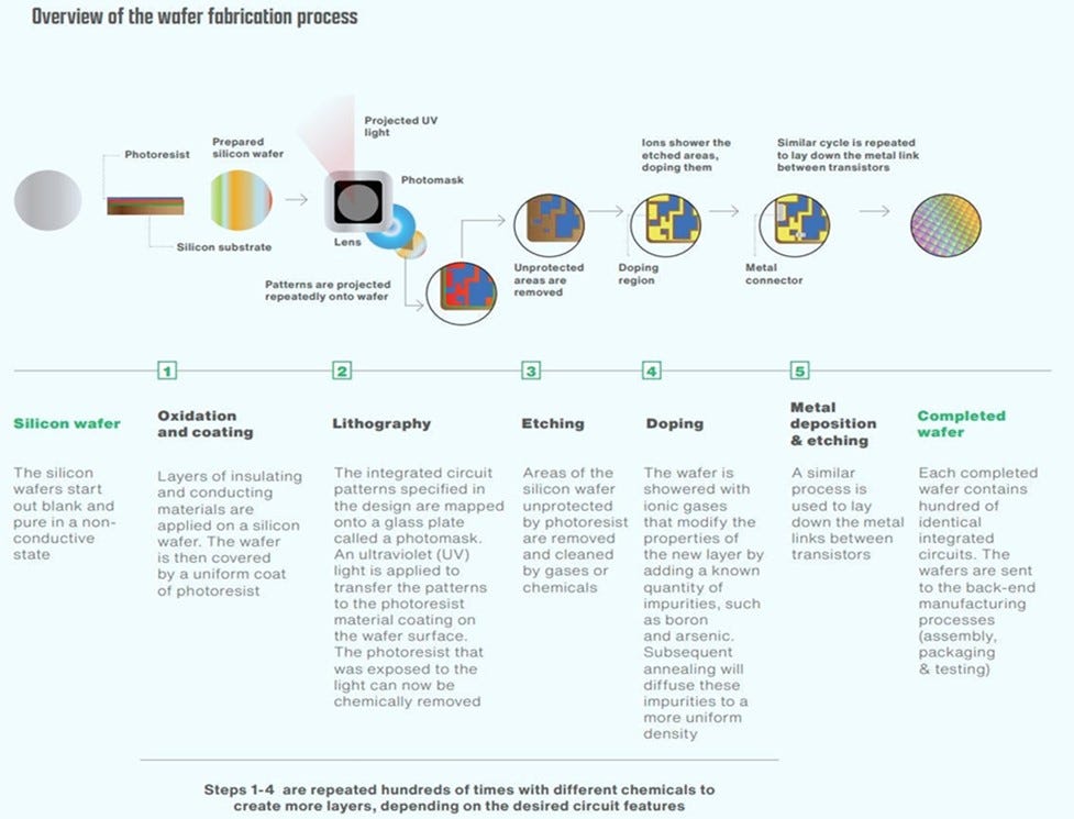
The diagram below shows the various stages of the wafer fabrication process. Lithography is one of the key elements in the manufacturing of chips.

Lithography (Stage 2 above) is using light in a complex way to print small patterns on silicon. Photolithographic machines use light to etch integrated circuits onto silicon wafers. The lithography tool draws the thinner and thinner lines that allow chips to shrink and become more powerful.
The dominant supplier (90% share) of the large, very complex and expensive lithographic machines is ASML of the Netherlands.
In 2019, ASML introduced Extreme Ultraviolet (EUV) machines. EUV has much shorter wavelengths of just 13.5 nanometres (billionths of a metre). Shorter wavelengths allow the etching of ever smaller components which is critical as companies move to smaller nodes striving to keep pace with Moore’s Law.
EUV was introduced in 2019 and was a big advance on UV and quickly accounted for 45% of ASML’s revenues.
Intel was slow to see the potential if EUV and fell behind more prescient rivals.
“As we went through our stumble of not embracing EUV and failing at 7nm, this allowed the industry to catch up.”
“And as you see with Intel 7nm, we went through great steps to avoid the need for EUV. It produced deficient in power performance area and cost.”
“We were slow to adapt to the step up in capital intensity and this fundamental shift to a foundry model.”
There are three key elements of IDM 2.0:
1.Internal factory network.
“We intend to remain a leading developer of process technology and a major manufacturer of semiconductors and will continue to build the majority of our products in our factories.”
2. Strategic use of external foundry capacity.
However, for strategic reasons they will use some external foundries especially for their leading-edge chips.
“We expect to expand our use of third-party foundry manufacturing capacity, which will provide us with increased flexibility and scale to optimize our product roadmaps for cost, performance, schedule, and supply. Our use of foundry capacity will include manufacturing for a range of modular tiles on advanced process technologies.”
Currently about 30% of their chips are manufactured by outside companies. Their stated long-term aim is to bring the share down to about 20%
3. System foundry.
This is the 3rd party manufacturing unit. A kind of mini-TSMC residing inside Intel.
“We are building a world-class foundry business (IFS) to meet the growing long-term global demand for semiconductors. We plan to differentiate our foundry offerings from others through a combination of
leading-edge packaging and process technology,
committed capacity in the US and Europe available for customers globally ( hedge against Taiwan risk for customers) and
a world-class IP portfolio that will include x86 cores, as well as other ecosystem IP.”
“The current foundry model enabled explosion of ecosystem innovation at the wafer level. This established model has historically served the industry well, but a new mindset is needed now.”
“We are building out a system foundry that has four components:
wafer fabrication,
packaging,
chiplet standard, and
software.
“The system foundry involves engaging with customers at multiple levels, from basic wafer manufacturing to helping define and implement their desired system architecture.”
“We intend to build our customers' silicon designs and deliver full end-to-end customizable products built with our advanced packaging technology.”
Financial Reporting
As part of the implementation of IDM 2.0, Intel will report under two segments going forwards. These are Products and Foundry Services. The latter is the manufacturing part of the company. In April 2024, Intel presented historical numbers as if the new split had already been in in place. This means the profitability (or lack of it) of the manufacturing unit was disclosed for the first time
“We now organize our business as follows:
▪Intel Products:
▪Client Computing Group (CCG)
▪Data Center and AI (DCAI)
▪Network and Edge (NEX)
▪Intel Foundry
▪All other
▪Altera
▪Mobileye (Now sold off)
▪Other”
Some of these restated numbers are shown below:
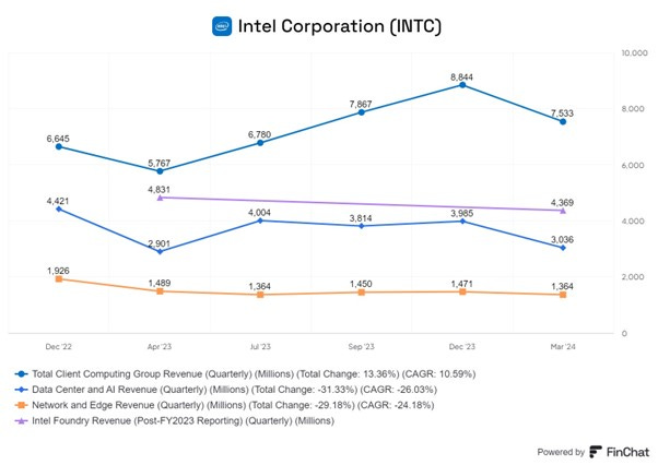
In terms of revenue, foundry revenue is at a run rate of ~$ 4bn per quarter while Products (Client computing, Datacentre and Network/Edge) is much larger at about ~$12bn per quarter.
“It's the first time you have had the information needed for an apples to apples compare with external fabless peers. Now that Intel Products has better visibility into what is really driving their costs, we see a clear opportunity to drive those businesses collectively to approach 60% gross margin and 40% operating margin.”
“the recast doesn't change consolidated results, and the elimination effectively adjusts for the intercompany activity between Intel Foundry and Intel Products. If you look at Intel Products, the 10% operating margin that we showed in the allocated cost model increases to 24% in the fair market price model, solidly profitable at this point in the cycle.”
“In fact, despite a significant drop in revenue, operating margin was flat year over year in 2023, really a testament to both the austerity measures we took as well as the very early progress identifying structural cost savings in the new model.”
We can look at the breakdown of operating income by quarter as shown below:
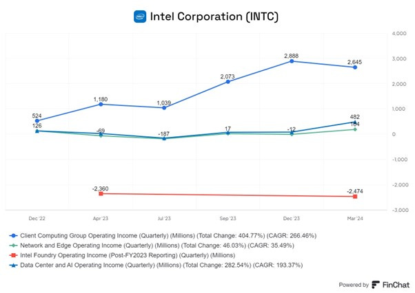
The key thing is the Foundry division (IFS) is loss-making at the operating level while the Product segment (especially client computing) is profitable.
“Our prior operating model allocated the cost of Intel Foundry into the product businesses, obscuring the underlying economics of both.”
“The new model creates a foundry relationship between our manufacturing assets and our product groups, whereby Intel products will now purchase wafers and services from Intel Foundry at a fair market price.”
“The fair market wafer price becomes a major revenue driver for Intel foundry and shows up as cost for Intel products. Similar to how fabless companies purchase wafers from their foundry partners, each group will then have the information they need to optimize cost and improve profitability.”
At these “fair market prices”, IFS is not profitable and this needs to be reversed.
One theoretical solution would be to spin off the foundry business completely and for the core Intel to become a fabless chip designer. This route has been rejected in IDM2.0
Progress Report on IDM2.0
The company gave a set of detailed presentations to present the progress made under IDM2.0 on
April 2, 2024, about four years into the project.
In their view, the key elements in IDM 2.0 are as follows:
1. Drive forward Moore’s Law
2. Embrace the Ecosystem & drive to Standard IP and practices
3. Optimise cost, efficiency and extended life of assets
4. Deliver internal and external products
Let us evaluate the progress they have made in all these areas
1. Drive forward Moore’s Law.
Their started aim was to have moved 5 nodes in 4 years.
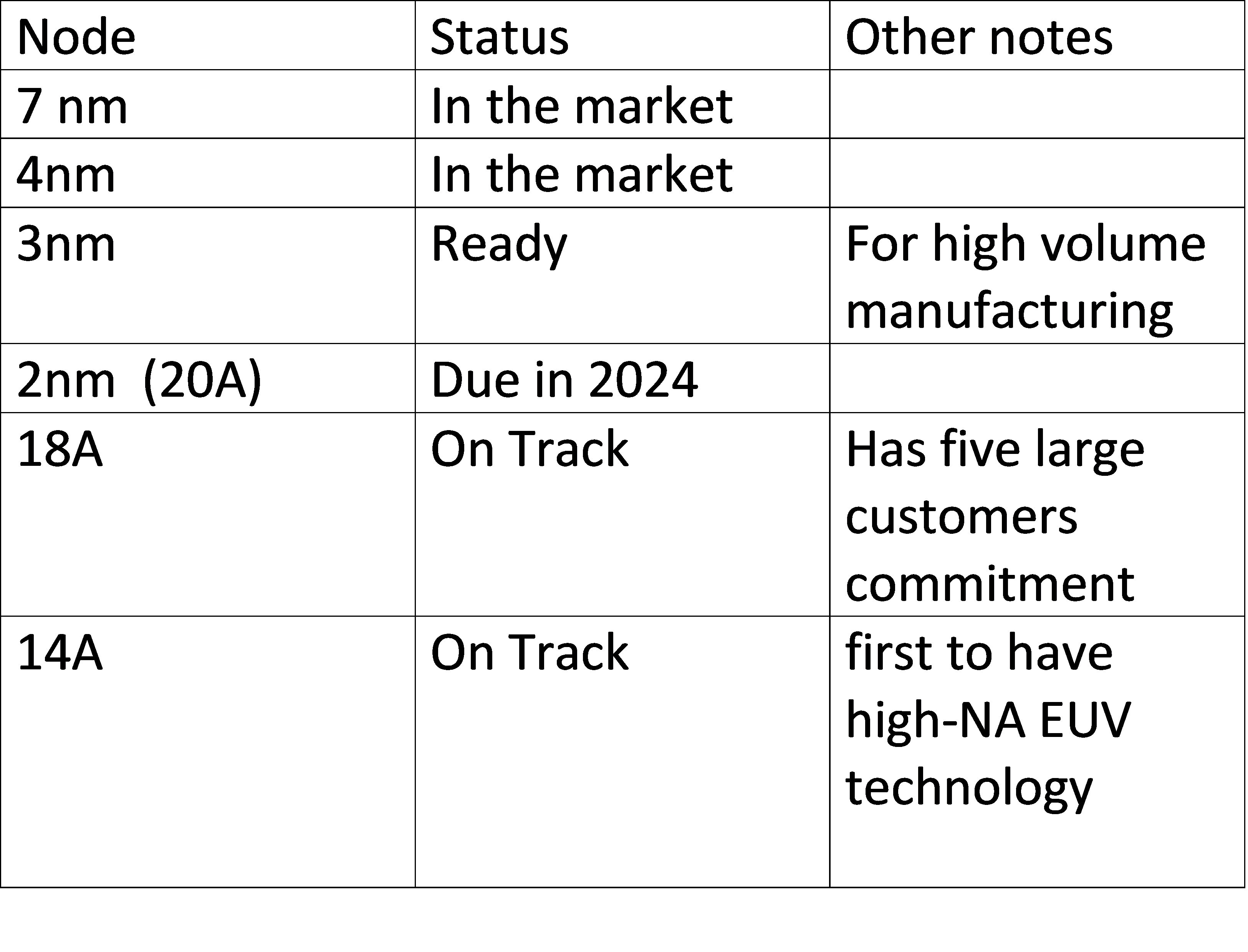
This has been a success; the company has put 7nm and 4nm chips in the market and is ready to work on 3nm and 2nm. The company can reclaim its place among the leading chip manufacturers in the world.
Intel 20A and beyond will be challenging. 18A is the equivalent of 1.8nm. Samsung and TSMC are working on 2nm. Therefore, if Intel can succeed at 18A, it will be the clear leader. The early adopters of 18A could be large-scale CSPs and hyperscalers, as well early collaborator, Microsoft. These entities aren't legacy chipmakers and are initiating new chip design programs, which bodes well for potential future business for IFS.
The more important test will be the 14A (i.e 1.4 nm) which if successful will clearly signal that Intel is ahead of TSMC and Samsung. More details on this can be found here
2. Embrace the Ecosystem
One of the reason Intel’s efforts at making 7nm chips faltered and led to the loss of several high-profile contracts was Intel’s failure to use the standard industry ecosystem.
The semiconductor industry's shift towards fabless operations necessitates a deep understanding of the EDA ecosystem and the complexities involved in porting designs to fabrication.
Intel now has partnership announcements with leading Electric Design Automation (EDA) companies: Cadence Synopsys and ARM. We covered EDA in our note on Cadence which can be found here
These partnerships are designed to enable industry standard design tools (EDA tools) and workflows such that customers can use industry standard process development kits (PDKs) to build their silicon designs.
As part of the policy of opening and embracing the ecosystem, the company is inking agreements with several types of companies including CSPs (AWS and Azure etc). IP owners (ARM, Rambus etc) and others.
3. Optimise cost, efficiency and extended asset life.
To compete and earn an acceptable financial return, INTC is trying to cut costs and extend asset life.
The key priority is to make the foundry business profitable at the operating level. Foundry is a capital-intensive asset-heavy and currently loss-making business.
Intel states that it has greatly improved its operating profit at IFS, and it is now on a path for reaching breakeven in the next few years.
Intel aim is for IFS to generate $15bn of external revenue by 2030.
Intel Foundry should be in the high-30s gross margin and high 20% operating margin.
How are they going to improve performance in IFS?
Intel has identified key drivers of profitability. These are
transistor leadership,
internal product mix and scale and
advanced packaging
Transistor Leadership. As they sell more and more of the most advanced chips, they will be able to raise prices more than the average.
“As we mix towards Intel 18A. We'll see meaningful Average Sales Price (ASP) uplift as well as a more competitive cost structure, which will drive improved profitability.”
Internal mix and scale. As the foundry starts to operate as an independent profit centre rather than a captive unit of the product team, it will remove certain operational inefficiencies which plagued the previous structure
One example of this is “Expedites”. Semiconductor manufacturing is an extremely precise process that requires wafers to move through the fab at very specific intervals.
As a captive unit of the Product teams, the foundry was often told to halt some process to expedite some other work which was important to the product team. Expedites interrupt the process, and a pure-play foundries such as TSMC charge a very steep premium for them and fabless companies use them sparingly.
Under the old structure, Intel product team requested expedites as a common course of business and manufacturing teams put capital in place to accommodate that inherent inefficiency.
However, as Intel has put in market pricing, IFS can charge the product teams the true cost of the expedite
“Since introducing market-based pricing last year, we've already seen a 95% reduction in expedites, with fair market pricing driving better decision making. We're also already seeing 5% to 10% improvement in capital per wafer start on new capacity, driving improved cost structure for the business.”
Market based pricing is leading to other cost efficiencies
“I talked about product design decisions changing under the new segmentation, and we're seeing this change manifested in a 75% reduction of test times for our next generation client product, again driven by the introduction of market-based pricing. We've also realized a greater than 10% reduction in engineering sample requests as product teams see direct charges from Intel Foundry.”
As we have emphasised in these reports, semiconductor manufacturing is very complex and highly capital intensive. The capital intensity increase as Chips become more advanced.
This means operating at scale with a high degree of capacity utilisation is critical for the profitability of manufacturing operation.
As Intel lost its product technical leadership, it saw a fall in demand as it could not supply the leading-edge chips. Therefore, capacity utilisation and profitability fell.
“An added benefit of improved transistor performance is increased demand for those transistors. Intel Foundry lost Intel products tiles to external suppliers due to the process deficits we discussed.
“As Intel Foundry regains process leadership with AT and A, it has already won future Intel product tiles, which increase scale. We think there's roughly 2 nodes worth of volume that will move back into Intel Foundry.”
“We have a number of external Foundry customers that we've signed up to drive increased scale for the business. As we increase scale, that improves utilization and ensures we can deliver a return on the capital we're investing.”
“Importantly, many of the drivers to breakeven are fully in our control and somewhat independent of revenue growth. Although it's always important in a fixed cost business, faster revenue growth allows us to achieve our targets more quickly.”
Profitability will be he helped by an increase in the period over which assets are depreciated.
“In reality, we've moved the depreciation to 8 years. I wouldn't envision us changing that going forward. Of course, we'll evaluate it on an ongoing basis, but there's no doubt that we will get longer use of the assets. It might not be reflected in the depreciation schedule, but it will be reflected in the return on invested capital and the return on assets.”
“Between now and then (2030), we'll hit breakeven operating margin about midway through that and then driving operating margin improvement through the period.
Leadership technology, stabilizing investment, cost and capital efficiencies, these are the tools to accomplish that financial outlook.”
The next chip they are working on is the 18A.
“We already have 5 customer commits and almost 50 test chips underway for 18A.”
If IFS can be profitable it will significantly improve the overall consolidated performance of Intel.
“There is meaningful value creation as we execute on this path to breakeven. Had Intel Foundry been breakeven in 2023, we would have added more than $1.40 to EPS, more than doubling our reported EPS for last year.”
It is hard to evaluate how much progress they have made to make IFS profitable. They are talking about achieving it by 2030. Clearly this is a long-term project, and it will not be easy as they will have compete with TSMC, Samsung and Global Foundries.
Intel will need to win business from fabless players to make its IDM 2.0 foundry strategy work. Otherwise, they will not have enough scale/volume to compete given their internal product business will continue to lose market share for the next few years. It isn’t possible to run a leading-edge foundry without multiple large, leading-edge customers.
5. Deliver internal and external products
There are two aims here.
· The first is to develop new products internally, which they have.
· The second is to persuade third party fabless and other companies to use INTC as their external third-party manufacturer.
Intel manufacturing capacity has expanded greatly and is set to do so further over the next five years.
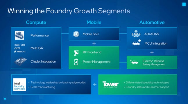
In Q1 2022, Intel acquired Tower Semiconductor Ltd. Tower was a leading foundry for analogue semiconductor solutions. They have a business in making lagging edge chips. Tower’s business profile is summarised below
Tower is the fab partner for many larger IDMs through various JVs. Panasonic is Tower’s largest customer at ~25% of revenue, but there are 5 additional customers that account for 4-11% of sales.
Intel believes adding Tower’s capacity completes their third-party foundry offering.
“This combination of leading edge and specialty technologies will position us as a truly global end-to-end foundry.”
“When we launched IFS last March, our customers were overwhelmingly excited to work with us. One of the things that consistently asked me was to add specialty and mature nodes to our portfolio. With Tower, we can honour that request and more broadly serve key market segments.”
Tower has standard workflows and a more customer-centric fab culture, and this could be a huge kickstart to creating a standard workflow at IFS.
Intel will benefit from that decades of experience that Tower brings and how to run a global foundry customer-centric business for our customers for the future.
As the slide below indicates they are planning to attack the Server/PC market (Compute), Mobile and Automotive. Tower has some strength in the latter
The economics of new capacity has also been changed as governments, led by the US, are giving huge subsidies to new manufacturing operations set up on their soil.
Intel has noted they are benefiting from the following:
· $8.5bn in grants,
· $ 11bn in loans and
· $ 25bn in tax incentives and
· EU grants worth $10bn +.
These subsidies will reduce capital spend, improve depreciation and ultimately improve their cost structure.
They have invested significantly in recent years to advance 5 nodes in 4 years.
In 2022, Intel announced two leading-edge factories in Ohio which will cost US$ 20bn and these will establish an advanced semiconductor campus in the “Silicon Heartland.”
Intel have announced $20bn investment in two new manufacturing facilities in Arizona, set to come online for production in 2024. These new fabs will be on leading edge process node technologies, with Intel extending cooperation with the State of Arizona, as well as the current administration’s target of improving semiconductor manufacturing inside the country. Intel also unveiled plans to build a Euro18.7bn factory in Magdeburg Germany for making cutting-edge semiconductors in the EU.
As we mentioned in our piece on TSMC here, Samsung and TSMC are also taking advantage of US subsidies to make significant chip manufacturing investments in the US.
Intel will be seeking to outfit its production facilities with the equipment necessary to enable leading edge manufacturing, including using Extreme Ultra Violet (EUV) technology.
The machines that enable EUV manufacturing are only supplied by a single company, ASML, and demand for these machines is at a record high, with a waiting list of over a year.
Intel has stated it has plans to add new plants in Arizona and Ohio in addition to the ones it has already announced. Intel has plans to invest up to Euro 80bn in EU in the next decade This will consist of
· a fab mega-site in Magdeburg Germany,
· a new R&D hub in France and
· manufacturing and foundry services in Ireland, Italy, Poland and Spain.
In addition to government subsidies. INTC has come up with a novel funding structure for large Fabrication investments. This is called Semi-conductor co-investment programme or SCIP.
The first SCIP is an equity partnership with Brookfield Asset Management called Arizona Fab LLC and will invest up to $ 30bn in the expanded manufacturing infrastructure in Arizona. Brookfield will provide 49% of the equity investment and Intel will provide 51%. Brookfield is a leading infrastructure investor.
“The whole SCIP structure is to essentially have Intel pay the equipment and our partner pay for the infrastructure and us to in a joint venture way drive the business, pay for the investment out of the profits of the factory. That's the simple way of thinking about it. And that's what we did with Brookfield. That's what the structure with strategically is trying to do with Apollo.”
The SCIP reduces the upfront investment that Intel has to make and de-risks the project but obviously this comes at the cost of dilution.
Intel has told investors that it expects that as much as 30% of its planned spending on new plants and equipment will be provided by government subsidies.
Intel is trying to turn competitors into customers, a strategic pivot exemplified by its recent collaboration with ARM. This partnership aims to provide cutting-edge foundry services for Arm's system-on-chips (SoCs), presenting a significant opportunity for both companies to support startups. By offering essential IP, manufacturing support and financial assistance, Intel and Arm aim to foster industry growth and innovation. Given that 80% of the wafers that TSMC runs have an ARM processor, it's clear that being in the foundry business means doing business with ARM.
Intel has announced that it will work with customers to build Chips with its own x86 architecture as well as ARM architecture and open-source RISC-V cores. The company will also be able to leverage Intel’s IP portfolio of core design and packaging technologies.
Their improved ability to manufacture leading edge chips is leading to new customers. Intel has a number of packaging technologies it could offer to 3rd party customers.
“Packaging Definition: Traditionally completed near the end of the manufacturing process, chip packaging is the arranging and installation of a chip with its electrical and protective components on a “substrate,” or base plate, made of silicon or other materials.”
Advanced packaging is also useful when a chip is operating within strict physical limits. Chips used in smartphones are a good example, because logic chips cannot get much smaller, and smartphones cannot get much bigger.
In 2017, Taiwanese chipmaker TSMC, together with Apple, introduced an advanced packaging technique called Integrated Fan-Out. This involves integrating logic and memory chips closer together through a new high-density “redistribution layer”, improving performance while removing the need for a thicker base layer.
What are the implications for the industry? Advanced packaging requires greater co-operation between industry specialists.
TSMC, for example, which has no background in memory chip production, works closely on Nvidia’s AI chips with memory market leader SK Hynix, which has no background in logic chip production.
Intel ands Samsung, meanwhile, have a record in both logic and memory as well as advanced packaging, meaning they will potentially be able to offer customers integrated services across all three areas.
The growth in importance of advanced packaging also offers an opportunity for second-tier chipmakers and traditional packaging companies, all of which are investing in their own advanced packaging capabilities, to gain a larger share of the $500bn semiconductor market.
Importance of Advanced Packaging.
Advanced Packaging Is likely to be a Key Driver of IFS Growth according to Intel.
It believes its s advanced-packaging technology prowess will be more important than ever in the era of AI chips.
“Moore's law is slowing, so design, manufacturing costs for leading edge nodes keep rising. Chiplet packaging, multi-die packaging and new advanced packaging will become distinguishing factors for chip companies that want to keep pushing the performance envelope.”
“Intel’s packaging portfolio continues to stay at the leading edge and at par with peers. This will be a key launchpad for driving differentiated foundry offerings for potential customers. Initially, packaging might be the gateway for potential foundry customers at the leading edge.”
Intel is already claiming some success in its quest for external customers
“We already have 5 external customers committed to 18a.”
“2024 is the trough for foundry operating losses. We've committed to being the number 2 foundry by the end 2030. The target date of breakeven profitability to be achieved in IFS is also 2030.”
Monetize leadership through both Intel Products and Intel Foundry Services (IFS)
This essentially states Intel will seek to make money from both of its divisions. The evidence for this will be in the numbers going forward.
Intel’s current use of 3rd Party Foundries.
Intel makes heavy use of external partners, such as TSMC, and already spends more than $7bn at TSMC annually.
Why use external foundries?
“ We use it for some specific nodes that we don't necessarily have for some capacity balancing. And in the cases, they're just capable of things that we haven't necessarily yet added to our foundry portfolio. These are important relationships for Intel, and part of being an Intel product and an Intel foundry, the products team will take continued use of them for as far as we can see into the future.”
This includes developing its leading-edge products on external foundry offerings. As Intel moves more into a chiplet ecosystem (Intel is calling it ‘tiles’), the company is prepared to manufacture its high-performance computing chiplets on external foundries.
Using external partners like TSMC, Samsung, Global Foundries, and UMC, will allow the company to optimize roadmaps for cost, performance, schedule, and supply.
“Chiplet Definition: A chiplet is a small, modular chip that performs a specific function very well. For example, a chiplet can be a processor core, a memory block, an I/O driver, or a signal processing unit. A number of optimised chiplets can be assembled together to replace one chip. ”
.
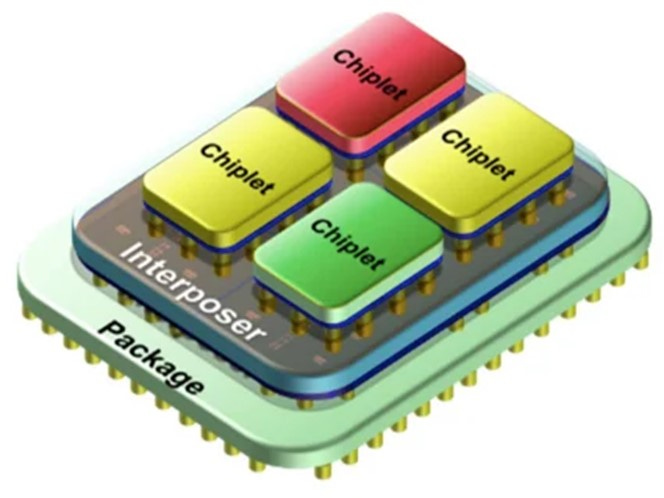
Image above shows 4 chiplets packaged to replace a single chip
Chiplets are a new way to build system-on-chips (SoCs) that can improve yields and reduce costs by more than 45%. A Chiplet partitions the chip into discrete elements and connects them with a standardized interface, allowing designers to meet performance, efficiency, power, size, and cost challenges.
“..this idea of chiplets allows us to even make greater use of Moore's law. We're able to, earlier in their life, have smaller die, which makes the process technology available for server and AI chip designs, also using less of the dye for IO and analogues for more efficient use of leading-edge technology overall.”
Chiplets were introduced in 2017 and Intel, unlike AMD (with Ryzen in 2017), did not initially embrace them. It is now playing catch-up.

Above diagram form AMD shows a hypothetical traditional monolithic chip (32 Core) compared with four chiplets. The overall result with the chiplet is much higher number of products. The placing of the four chiplets into the single unit is called packaging and it is a highly advanced product.
https://www.nextplatform.com/2021/06/09/amd-on-why-chiplets-and-why-now
Intel is trying to turn competitors into customers, a strategic pivot exemplified by its recent collaboration with ARM. This partnership aims to provide cutting-edge foundry services for Arm's system-on-chips (SoCs), presenting a significant opportunity for both companies to support startups. By offering essential IP, manufacturing support and financial assistance, Intel and Arm aim to foster industry growth and innovation. Given that 80% of the wafers that TSMC runs have an ARM processor, it's clear that being in the foundry business means doing business with ARM.
Apple's new M4 chip, an ARM-based AI PC processor with 38 trillion operations per second (TOPs), is likely to stoke competition among x86 incumbents Intel and AMD, as the race to pass 40 TOPs drives faster adoption of AI PCs. You can read about the specifications of the M4 here.
Qualcomm's ARM-based PCs remain a threat to x86 AI PC goals. Nvidia is working on an ARM based CPU. The imminent widespread introduction of AI PCs sould lead to higher growth in PCs for Intel.
Some aspects of Intel’s current situation
The company claims to have fundamentally changed their culture. Cultural change is difficult to achieve and any claims of it must be taken with a pinch of salt. Intel clearly needed a cultural change irrespective of how hard it would be achieved.
Pat Gelsinger has made a lot of changes.
He has completely reorganised the business units and changed the financial segment reporting in a fundamental way.
He increased hiring in a major way to counter the previous regimes aggressive cost cutting-driven shrinking.
He increased stock-based compensation for critical design and fab employees. These are the people who will have to drive the manufacturing business to profitability.
Intel’s components research and long-term development teams responsible for process node development had a massive increase in resources. They were given more personnel and pay with a much better management structure.
“First, we're rebuilding that (Andy) Grovian execution as we call it, bringing back that heart of Andy Grove, the confidence, the engineering centricity, the discipline, the competitive spirit.”
“We've leaped forward with our embrace of EUV. We've built deep partnerships. We used to tell the equipment vendors, drop it on the shipping dock and we'll take care of it from there.”
Intel had been the leaders of manufacturing for so long that they had, perhaps understandably developed a superiority culture., Intel’s fabs though they knew better than even their equipment vendors who were critical technical and business partners.
An example of this lies in Intel failure at the 7nm and 10nm node. These were a major failure which had many causes. One was related to equipment supplied by Applied Materials (AMAT) that Intel wanted to use for a particular process. They were wanted by AMAT that their equipment was not ready but the process. Intel thought they knew best, pushed ahead with their plans and this caused massive issues which took years to rectify.
Intel has recognised its mistakes, has fired people thought to embody the old toxic culture. There is now much greater respect for Intel’s suppliers.
“Now we're deeply partnering with them. And in particular, the ASML relationship is superb. We rebuilt the leadership team.”
In the 2010s, tool vendors did not like Intel that much. The tool vendors understand where their tools are being used, how they are used. Working closely with tool vendors is incredibly important. ASML is helping Intel learn how to ramp EUV, they are shipping them a lot of EUV tools to multiple fabs, and they are even giving intel the first production High NA EUV tool. This preferential treatment is also being given to Intel by other vendors by Intel.
Intel will be the first, by a margin of years, to adopt ASML’s high-NA EUV lithography scanners in high volume manufacturing. Both TSMC and Samsung have only ordered tools for R&D. Intel, perhaps trying to correct for being late to the low-NA game, has been high-NA’s loudest and strongest champion.
Definition. High NA is High Numerical Aperture. High NA lithography “provides the ability to dramatically improve resolution and feature scaling for the next generation of processors, enabling Intel Foundry to continue process leadership beyond Intel 18A.”
“We're leveraging the expertise not only of the equipment industry, but the EDA industry and moving to industry standard design tools and PDKs. And those of you who might talk to industry and equipment vendors, they will resonate. This is a new Intel, more open, engaged, and proactive than ever before.”
A key change has been the re-introduction of OKRs (objectives and key results) which was an important framework to track goals and outcomes which had been implemented by Andy Grove.
“We brought back OKRs,. Why do we stop doing that? We invented it. Everybody else in the Valley embraced it, and we stopped doing it, we are doing it again. We've tied every person in the company and part of their financial rewards is based on their OKRs, and their individual execution against them. The culture is being rebuilt.”
Intel : A financial snapshot
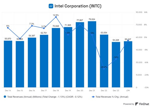
Annual Revenues peaked in 2021 and have declined meaningfully since then. Total Revenues fell after peaking in 2021 as Intel failed to make the leap from 10nm to 7nm manufacturing and this led to a loss in market share to rival such as AMD. The latter was able to outsource production to TSMC and to leap to 7nm.
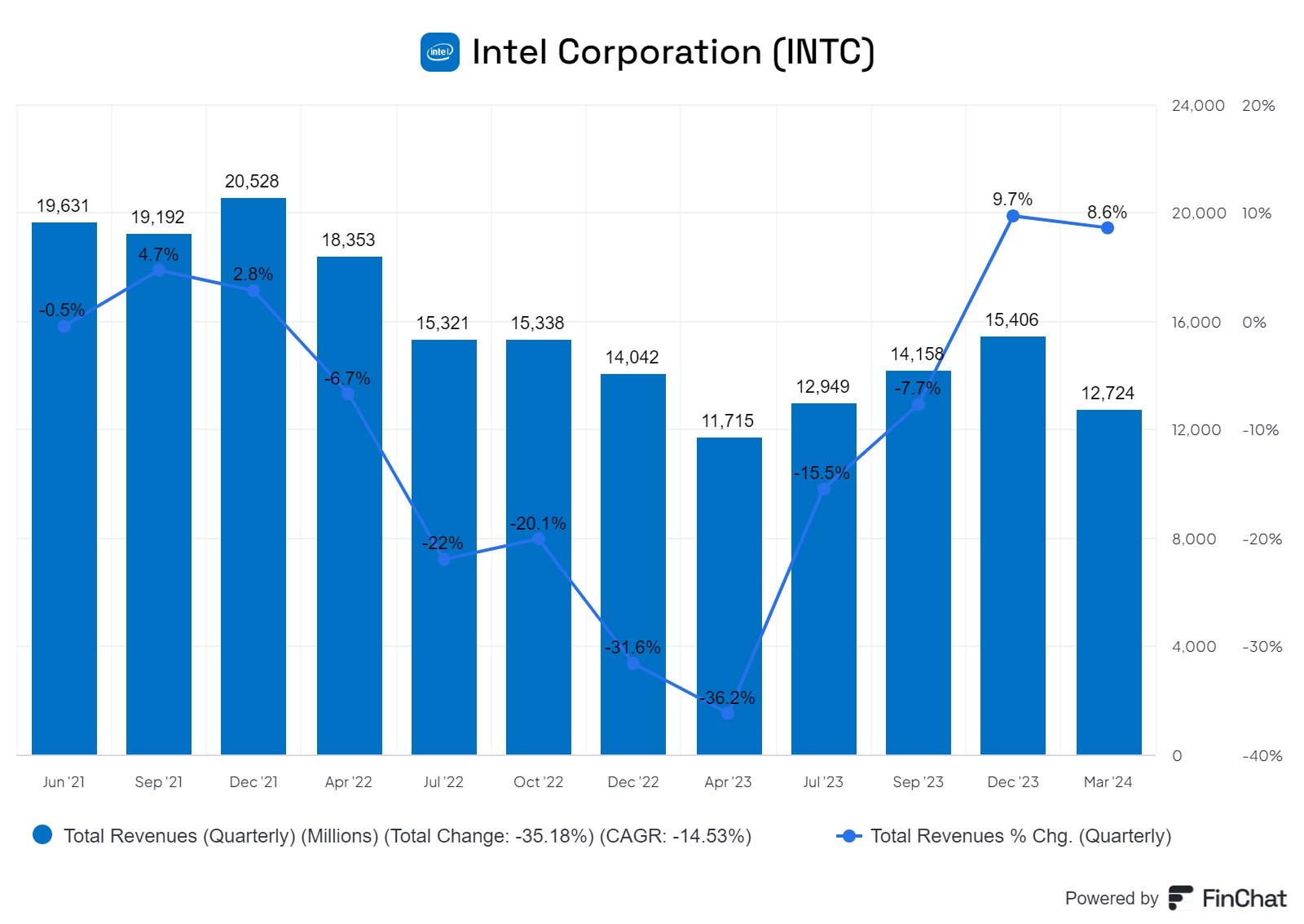
On a quarterly basis we can see the decline quarterly revenues from 2021 to 2023.
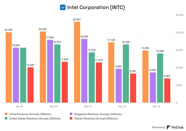
The geographical breakdown of INTC demand reflects the location of the manufacturers of Servers, PCs and Laptops with China, Taiwan and USA prominent.
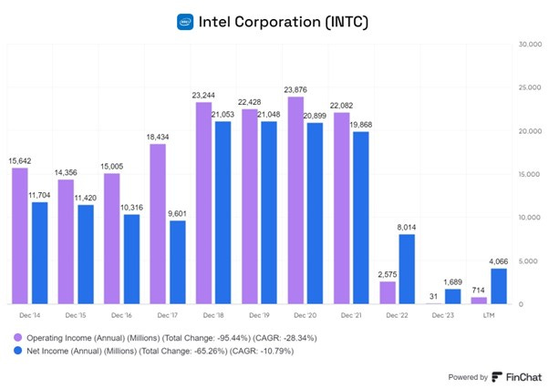
Operating Profit and Net Profit fell in 2021 as the decline is revenues fed through to profits in a disproportionate way reflecting the high fixed costs of the business.
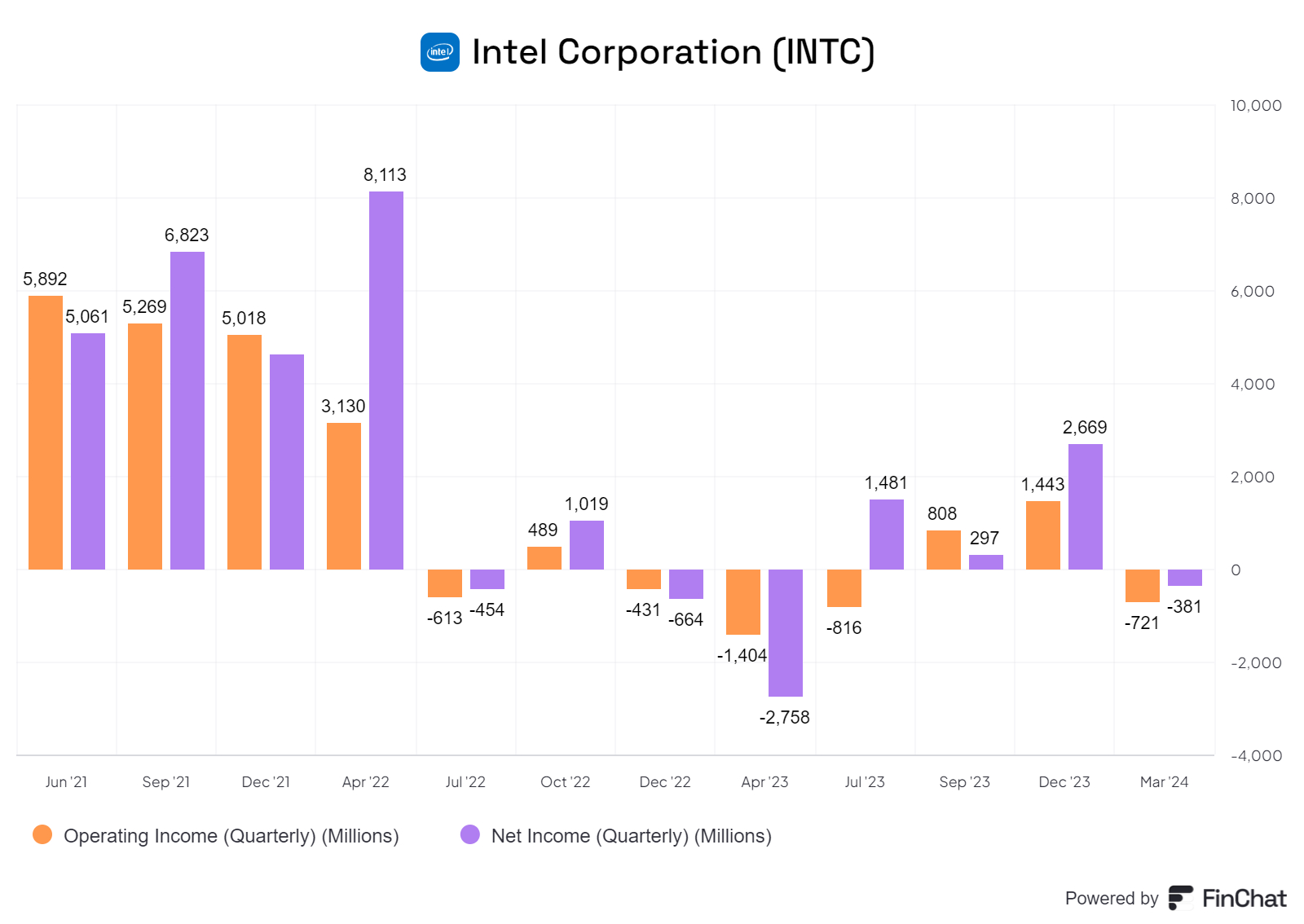
Quarterly profits have fallen sharply since 2021.
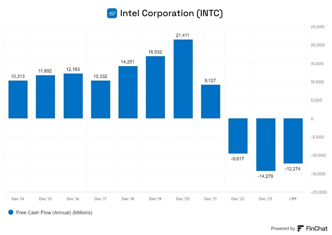
Free cash flow became negative from 2022 onwards
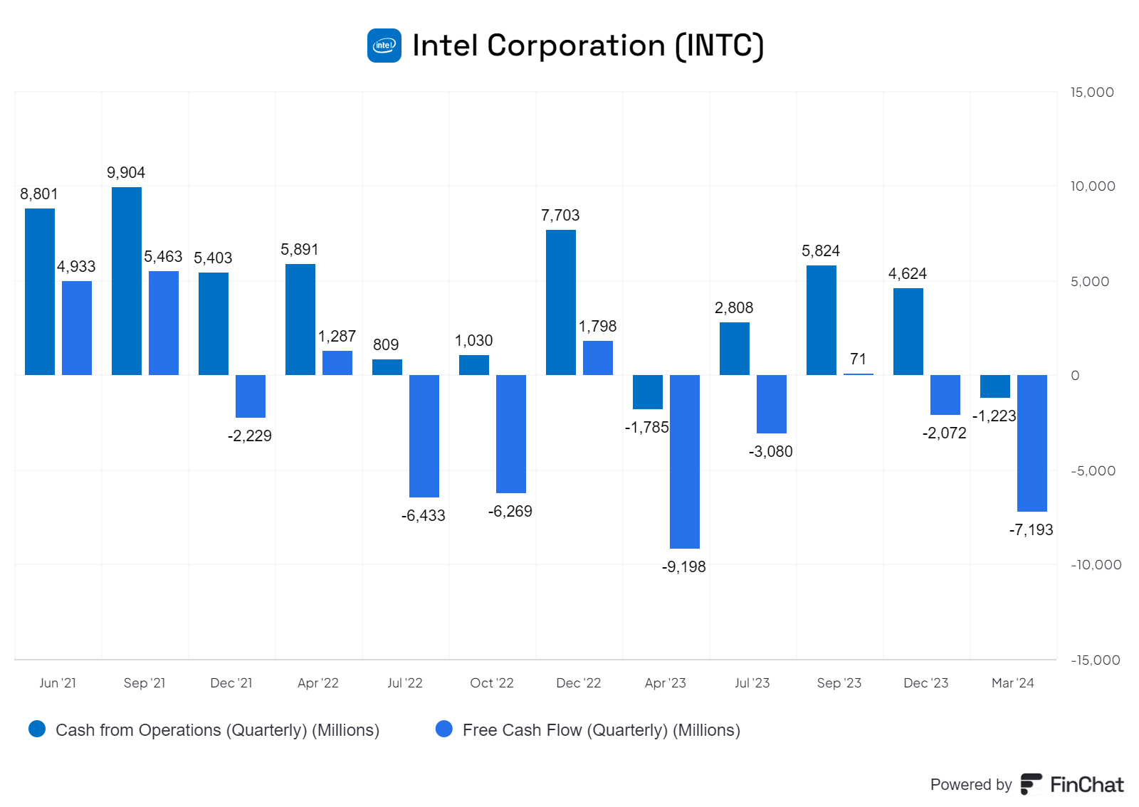
On a quarterly basis, we can see free cash flow has been negative since 2021.
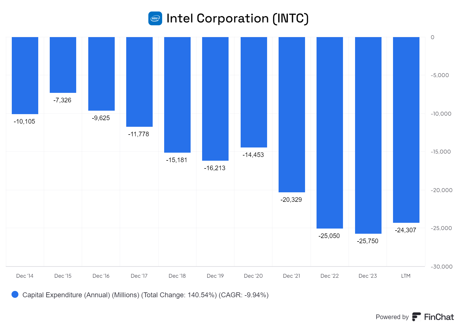
Capex has increased greatly since 2020 as the company has invested greatly to catch up fur nodes and be in the position to manufacture 3nm chips. This has been largely successful. It has increased from an annual run rate of $ 14bn to $25bn
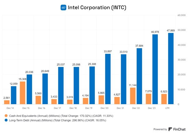
The high capex has been funded by partly by operating cash but to a greater extent by increased long-term debt. The latter has increased from $ 25bn in 2019 to about $ 48bn currently
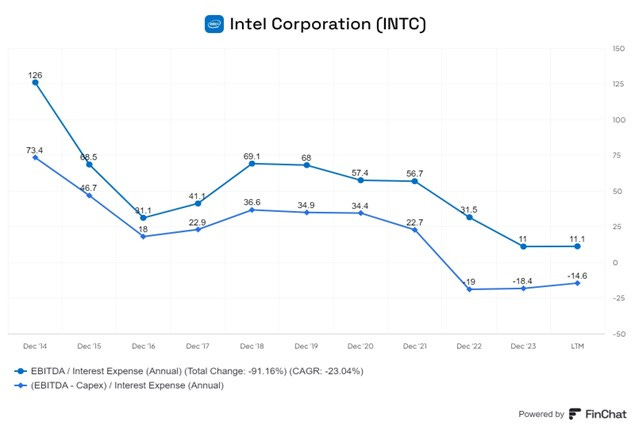
As a result of the higher debt, interest coverage has fallen as shown in the chart above. EBITDA /Interest Expense ratio has fallen from 57 times to about 11 times. Interest cover is still healthy but there is little room for significant further debt issuance.
Design has much higher margins than manufacturing. Nvidia, for example, has gross margins between 70~65%,. Intel once had margins somewhat closer to Nvidia’s but these have fallen a little in recent years.

Operating margin and Net margin fell sharply post 2020, due to a decline in the top line and the greater investment required in leadership products.
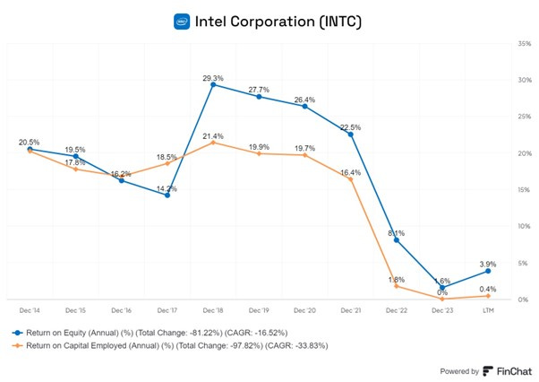
The profitability of the company fell from 2002 with RoE declining from about 27% to ~4%.
Summary
Intel has been central to the history of the Chip industry
It was founded by Robert Noyce, the inventor of the Integrated circuit (IC) and Gordon Moore who are articulated Moore’s Law which proved to be remarkable forecast about the progress of the speed of chips for five decades.
Manufacturing and Engineering at Intel was run by Andy Grove who was a legend in in the industry.
With the x86 architecture, Intel become the dominant player in the supply of CPUs for PCs.
This position was consolidated in the 1990s with the Pentium branded Chips.
However, Intel missed out on the mobile revolution. The number of mobile devices exceeded computers and chips for mobile phones became a huge market that Intel missed out on.
Intel’s famed engineering prowess took a huge hit in 2020 when they failed make the leap from 10 nm to 7nm. They fell behind Taiwan Semiconductor (TSMC) and Samsung. Volumes fell and margins and profits declined drastically.
TSMC has pioneered a revolutionary 3rd party manufacturing company which later encouraged AMD to divest its foundry. It also encouraged the emergence of fabless companies such as Nvidia and Qualcomm.
Nvidia and Qualcomm have become major players in GPUs and Mobile chips respectively and AMD became a tougher competitor in CPU. Many companies, such as Apple, Amazon and Meta are designing their own chips while Nvidia is reportedly working on ARM-based GPUs. Competition for Intel will only get more intense, and Intel will not dominate newer markets in the way they dominated the
Intel could have spun off the manufacturing business. They have decided not to do so but continue with an integrated approach. However, the SCIP with Brookfield represents a step in this direction – it is a 50% spin off of one fab and more of these are likely to be done.
Under IDM 2.0, the company is breaking down the numbers into Products and Foundry for the first time. This shows the Foundry business is not profitable. The greater transparency should lead to greater efficiency and better metrics for IFS.
They key to recovery will be continued leadership in Products combined with getting more third-party volumes in IFS. Intel must be manufacture at scale for fabless companies and that will take capital, a deep cultural change and the ability to face up to the competition.
Valuation
The analysts’ consensus expectations for EPS in FY2024, FY2025 and FY2026 are at $ 1.10, $ 1.98 and $ 2.58 respectively. These are shown below.
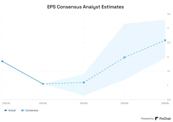
At the current share price of $ 31 per share, it is on a tree year forward P/E of 12 times. This indicates it is not too expensive. However, this assumes a strong recovery in earnings in the next three years and high earnings beyond.
Conclusion
Intel is a complex story with many moving parts.
They faced a huge setback in 2020 and are trying hard to recover from it.
Their substantial investments have paid off in the sense that they are once again manufacturing chips at the leading edge.
They have dual strategy of partially diluting their stake in the manufacturing processes while at the same time trying to make IFS profitable. This is going to be difficult and even the firm does not see this happening till 2030.
Intel’s recovery is a work in progress. We will continue to track it to see if there are signs of progress in the financial numbers. We are not allocating capital to it now.